LCD Voltage Inputs Explained
This note will briefly explain the various voltage pins available on an LCD. These voltage pins can be seen on character, graphic and TFT displays. As an example, a graphic LCD will be reviewed. The graphic display that will be discussed is a 128×64 dot transmissive graphic LCD. This is part number G12864B-BW-LW63. Please review the specification sheet of the display and the embedded display controller ST7565P for further details on this display.

Below are the names and definitions of the voltage pins that can be seen on this display. These pins are typical on graphic LCDs and these definitions are consistent between displays. The specification sheet of the individual display should be checked to verify the pin names and definitions.
| Pin | Definition | I/O | Connection |
|---|---|---|---|
| VDD | Voltage input pin. Typically, 3.3V or 5V (depending on the display). Needs to be applied externally to this pin. This voltage is used in the internal voltage boosting circuit that is available on the display. Options are available for the multiplication of this voltage that is boosted. This will also be used as the logic voltage for the display’s interface operations. | Input | Voltage |
| VSS | Voltage ground pin of the display. Connect to the ground of the input voltage VDD. | Input | Ground |
| VO | Voltage output pin. This is the output voltage of the voltage boosting circuit. This pin can be measured across VO and VSS as the stepped-up voltage that is used for the pixels on the display. This pin does not need voltage to be applied if using the internal voltage boosting circuit. The voltage boosting circuit can be turned on/off through commands to the display’s controller. Review the controller’s datasheet ST7565 for command definitions. If using the other voltage controlling circuits but not the voltage boosting circuit, voltage will need to be applied externally to this pin. If using the voltage boosting circuit, you can connect this pin to a capacitor into VDD or VSS. | Input / Output | Connected to VDD/VSS or external power |
| VR | Voltage regulator pin. The display’s controller IC contains a voltage regulating circuit that consists of an internal voltage divider. This pin will adjust the contrast of the displays pixels by increasing or decreasing the voltage of the booster circuit. This pin remains unconnected if using the internal voltage regulator. If not using the internal voltage regulator, resistors can be connected across VR and VSS and across VR and V0 to create an external voltage divider for the display. The internal voltage divider circuit is controlled by commands defined in the IC controller datasheet ST7565. | Input / Output | Open or Connected to resistors in an external voltage divider |
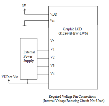
| V4-V0 | Stages of the voltage boosting circuit. These pins need to be connected to capacitors (1-2.2uF) to VDD or VSS when using the voltage boosting/regulating/following circuits. If not using these circuits, you will need to connect these pins to an external power supply at different voltage stages while maintaining the relationship: V0≥V1≥V2≥V3≥V4≥VSS. | Input / Output | Capacitor or External voltage variant for each V0-V4 |
Pin Connections
The voltage pins that require a connection are VDD, VSS, VO and the V4-V0 while VR can be left open when using the internal voltage regulating circuit. Each of these voltage pins are a part of the internal voltage controlling circuits. The VO pin is the output voltage of the voltage boosting circuit. V4-V0 are the pins at each step of the voltage boosting circuit, with V4 being the first stage and V0 being the highest stage. The VR pin is for the voltage regulating circuit which consists of an internal voltage divider which can be set to adjust the voltage of the boosting circuit. If not using these circuits internally, an external voltage can be applied at these pins.
Some graphic displays will have on board capacitors available for the pins which require them. The display in this example does not and therefore external capacitors will need to be connected to the required pins. A reference of the voltage controlling circuits will show the pins that require the capacitors. VSS and VDD do not require capacitors and will always need to be connected to ground and voltage supply.
It is recommended to use the internal voltage boosting circuit to provide the different voltage levels of the pins V4-V0. Graphic LCDs require different voltage levels for the com and segment lines that generate the pixels on the display. Refer to the controller datasheet for details of the combinations of the com and segment voltages and their waveforms. If not using the internal voltage boosting circuit, you will need to apply different voltages to each of the V0-V4 pins.
V4-V0
The internal voltage boosting circuit can provide the voltages required for pins V4-V0 that meet the requirement: V0≥V1≥V2≥V3≥V4≥VSS. Otherwise you will need to provide these different voltages externally to meet these requirements.
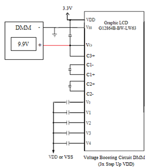
In the case that the voltage boosting circuit is used, the V4-V0 pins should be connected to a capacitor in the range of 0.1-4.7uF (depending on the size of the display) between each pin and VSS or VDD. Below is a reference of the required pin connections both with and without the use of the voltage boosting circuit.


The pin V4 will have the lowest voltage when measured across VSS when using the internal voltage divider. Pins V3-V0 will increase in voltage to meet the desired output voltage. The multiplier capacitor configuration circuits are specified in the datasheet of the controller. The highest voltage that is the result of the voltage boosting circuit will be at V0 and VO. This can be measured at each of the pins with a multimeter when connected across VSS.
VO
The VO pin, also known as Vout, is the output voltage of the voltage booster circuit. This circuit can increase the input voltage at VDD by a set multiplier which indicated by the connected capacitors. The multiplier can range from 2 to 6 times VDD. The choice in the multiplier value should be based on the value of the input voltage, VDD, and the voltage ratings of the display. The voltage that is stepped up from this circuit can be measured at the pin VO across VSS. Below is an example of measuring the stepped-up voltage VO at an input voltage of VDD=3.3V. The circuit and capacitor connections demonstrate a 3xVDD voltage boosting circuit.
The voltage can be measured across VO as the stepped-up voltage of VDD at the set multiplier by a digital multimeter. Additionally, you can measure the different voltage stages across each of the V0-V4 pins.

VR
The voltage regulator circuit controls the voltage boosting circuit, specifically V0. The VR pin can be left open when using the internal voltage regulating circuit. This circuit is programmed through commands which adjust the resistive voltage divider and the electronic volume function. This will adjust the contrast of the pixels on the display without the use of external resistors.
If not using the internal voltage regulator, an external voltage regulator can be connected through this pin, V0 and VSS. Below is a reference circuit of the internal and external uses of the VR pin.


DISCLAIMER
Buyers and others who are developing systems that incorporate FocusLCDs products (collectively, “Designers”) understand and agree that Designers remain responsible for using their independent analysis, evaluation and judgment in designing their applications and that Designers have full and exclusive responsibility to assure the safety of Designers’ applications and compliance of their applications (and of all FocusLCDs products used in or for Designers’ applications) with all applicable regulations, laws and other applicable requirements.
Designer represents that, with respect to their applications, Designer has all the necessary expertise to create and implement safeguards that:
(1) anticipate dangerous consequences of failures
(2) monitor failures and their consequences, and
(3) lessen the likelihood of failures that might cause harm and take appropriate actions.
Designer agrees that prior to using or distributing any applications that include FocusLCDs products, Designer will thoroughly test such applications and the functionality of such FocusLCDs products as used in such applications.