1. Introduction
The most common digital input voltages for displays and other electronics are five volts or three volts. Newer display technologies and the supporting electronics are shifting the required input voltage from five volts to the three volt input. This has to do with the internal semiconductors used to drive the displays which now require smaller digital input voltages. Having a lower input voltage is ideal for low power consumption and high speed signaling.
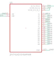
Converting the digital input voltage from a five volt source can be done through voltage level shifting. This will protect the display from exceeding the defined voltage tolerances and prevent damage to the internal display driver. The level shifting is done to every digital voltage signal supplied to the display. This application note will cover the details on level shifting input voltages for displays.
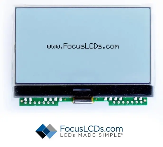
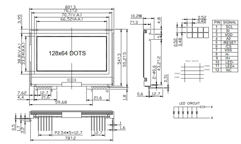
The display used in this application is a graphic LCD G126FLGFGSW64T33XAR with an input voltage of three volts. Graphic LCDs will commonly have an input voltage of five or three volts. The input voltage is specified in the datasheet of the display.
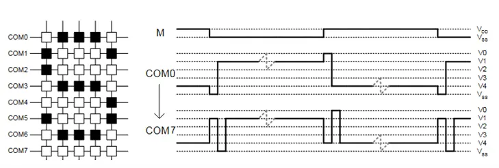
The voltage will be specified as a range of levels. The details of the input voltages are described in the datasheet of the display driver. The display driver used in this example is a graphic LCD dot matrix controller ST7565.
The voltages that will require level shifting will be the digital logic voltages that apply to the three wire serial communication interface. The voltage for the heater, backlight and internal voltage boosting circuit will not require level shifting.
For many graphic LCDs, there will be pins for capacitors and output voltages. These pins should not be level shifted because they require voltages that exceed three volts to be generated for the liquid crystal in the display. This note will review the voltage level shifting of five volts to three volts for the digital logic circuits of a graphic LCD.
Defining LCD Voltages
LCDs will have two voltages specified in the datasheet. One voltage, labeled as VDD, is for the digital logic used in signaling the display controller. The other voltage is used to create the various voltage levels seen as the contrast on the liquid crystal display. This voltage is typically defined as VLCD or Vout. The VLCD voltage will be used for the voltage follower, voltage booster and voltage regulating circuits.
The VLCD voltage is generally provided by the internal circuits of the display driver. The value is specified as the highest voltage level that the display will use to create the contrast of the liquid crystal. The pin specifications for the display G126FLGFGSW64T33XAR are reviewed in the table below with the standard graphic LCD voltages defined.
| No. | Symbol | Definition | Value | I/O |
| 1 | SCL | Serial interface clock signal | Digital input pin | I |
| 2 | SI | Serial interface input signal | Digital input pin | I |
| 3 | VDD | Digital logic input voltage | 3V supply | P |
| 4 | A0 | Data or command selection pin | Digital input pin | I |
| 5 | RESET | Reset signal of the display driver | Digital or analog high | I |
| 6 | CS | Chip select signal | Digital input pin | I |
| 7 | VSS | Digital logic ground | Ground | P |
| 8 | H- | LCD heater ground | Heater ground | I |
| 9 | H+ | LCD heater voltage supply | Heater supply | I |
| 10 | LED- | Backlight circuit ground | GND | I |
| 11 | LED+ | Backlight circuit voltage supply | 3.3V | I |
| 12 | NC | Not connected | NC | — |
I: Input, O: Output, P: Power
The voltage pins are defined in detail below. The digital voltage input is at three volts and is referred to as VDD. Pins 8 and 9 are the power supply for the heater of the display. The heater is used to support display applications operating in very cold temperatures. The different symbols used for these voltages are described in the final column.
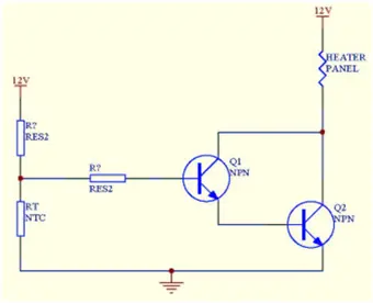
The connection between the LCD heater and the display panel are represented by the reference circuit. The heater panel is external from the voltage level shifting done in this application. The voltage supplied to the heater is 12V and will not be level shifted. The higher voltage should be supplied by an external source independent of the digital voltage and the backlight power.
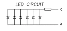
The backlight of the LCD should be used to illuminate the display and operates at 3.3V. The backlight should be powered externally from the level shifted voltage and externally from the heater circuit. The backlight LED circuit requires 50mA minimum to illuminate the LED circuit. This current is not provided at the output of the voltage level shifting circuit. Certain hardware integrations can power the backlight from the level shifted voltage but that will not be covered in this example.
Power and Voltage Definitions
| Symbol | Description | Alt. Symbols |
| VSS | Power ground for all digital circuits | GND |
| VDD | Digital logic voltage for signaling the display controller | VCC |
| VLCD | Voltage for pixel contrast. The output voltage will be generated internally. VLCD = 8.7V | VO |
| H- | Heater ground for the attached liquid crystal and circuit heater | — |
| H+ | Heater voltage for the attached liquid crystal and circuit heater | — |
| LEDA | External backlight power input voltage | A |
| LEDK | External backlight power ground | K |
Table 2: Graphic LCD Voltages
The voltages enabled in the internal voltage generating circuit are generated by the internal voltage boosting circuits. These voltages are created as levels for the liquid crystal to step from and are defined by the level VLCD.
The number of levels is defined by the voltage bias for each display. The voltage duty is the ratio of time that the liquid crystal is in the ON state for the multiplexed design. Below are the values of the duty and voltage bias for the graphic display used in this example.
| Symbol | Name | Description | Value |
| D | Duty Cycle | Duty cycle of the LCD. Defines the amount of time the liquid crystal is in the ON state. It can also be called the multiplex ratio. | 1/64 |
| 1/N | Voltage Bias | Voltage bias is the number of levels the display can step between when driving the LCD. The number of levels define | 1/9 |
Table 3: Voltage Bias and Duty Cycle
The voltage duty and bias are defined in the datasheet of the display. The voltage bias and duty are based on the number of pixels or dots that will be displayed. These values are selectable through the programmable interface of the controller. The bias voltage levels are generated from the input voltage at VDD.
These voltages are separated into the digital logic circuits and the power supply circuits for the voltage generating circuits. The digital logic voltage applies to the VDD power supply and the data and signal pins. If the internal power generating circuits are used, the VDD voltage will boosted and output at VO.
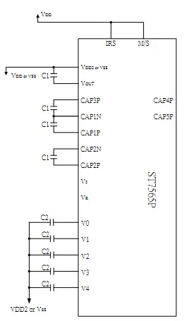
The voltage level shifting will only apply to the digital logic supply circuits. This includes the data lines and the VDD voltage input. In many cases, graphic LCDs will require external capacitors to be supplied to the display pins. These capacitors are used for the voltage booster circuit to create the voltage levels. These capacitor input pins should not be connected through the voltage level translator.
The voltage levels defined by V0, V1, V2, V3 and V4 may be available on many graphic LCD pin outs. These are each of the stages of the voltage boosting circuit and will be used as the levels for the voltage to step between. These voltages should not be connected to the level translator and will exceed 3.3 volts.
Hardware Definitions and Connections
The circuit used to shift the voltage levels from five to three will be reviewed in the section below. The required parts are described in the following table. The parts used can be replaced by the functional equivalent to fit the display application.
| No. | Name | Part | Description | Qty. |
| 1 | Voltage Level Shifter | SN74LVC4245APWR | 8-channel bidirectional voltage level translator | 1 |
| 2 | Voltage Regulator | LD2980ABM30TR | Linear voltage regulator 5V to 3V | 1 |
| 3 | Resistor | R0603 | 500 ohm resistor | 3 |
| 4 | Capacitor | C0603 | 5uF capacitor | 1 |
| 5 | Capacitor | 1uF capacitor | 1 |
Table 4: Component Selection
The voltage level shifter will require an input voltage of 3V to provide the level shift maximum for the digital logic signals. The voltage regulator is a five to three volt regulator that operates with very low current. The voltage regulator will be connected to the 5V power supply and output the 3.3V or 3V depending on the hardware configuration of the resistors and capacitors.
The voltage regulator has an on and off pin that will need to be connected to the five volt supply to enable the device. The enable pin can be used to turn on or off the voltage regulator which would also turn off the voltage level translator.
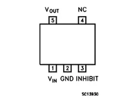
Below are the connections required for the voltage regulator.
| No. | Symbol | Description | Connection |
| 1 | VIN | Voltage input pin | 5V |
| 2 | GND | Ground | Circuit ground |
| 3 | INHIBIT | ON/OFF switch for the regulator | 5V |
| 4 | NC | Not connected | — |
| 5 | VOUT | Voltage output pin | Output 3V to Level Shifting Circuit |
Table 5: Voltage Regulator Connections
The voltage level shifting circuit will take the input signals that are operated at five volts and maintain and level them at three volts. This is important when connecting a three volt display with hardware that output five volts. This will protect the display from damage due to overpowering the device and display driver.
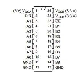
The voltage level translator can be used in both directions to shift from 5V to 3V or vice vera. This is ideal for graphic display applications because many graphic LCDs are available at both voltage supply inputs.
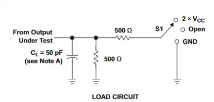
Below are the connections to the voltage level shifting circuit.
| No. | Symbol | Description | Connection |
| 1 | VCCA | Power supply input or output | Input 5V |
| 2 | DIR | Direction control A-B, B-A | 5V |
| 3 | A1 | Transceiver I/O pin | Digital logic input |
| 4 | A2 | Transceiver I/O pin | Digital logic input |
| 5 | A3 | Transceiver I/O pin | Digital logic input |
| 6 | A4 | Transceiver I/O pin | Digital logic input |
| 7 | A5 | Transceiver I/O pin | Digital logic input |
| 8 | A6 | Transceiver I/O pin | Digital logic input |
| 9 | A7 | Transceiver I/O pin | Digital logic input |
| 10 | A8 | Transceiver I/O pin | Digital logic input |
| 11-13 | GND | Ground | Ground |
| 14 | B8 | Transceiver I/O pin | NC |
| 15 | B7 | Transceiver I/O pin | NC |
| 16 | B6 | Transceiver I/O pin | Digital logic output to display |
| 17 | B5 | Transceiver I/O pin | Digital logic output to display |
| 18 | B4 | Transceiver I/O pin | Digital logic output to display |
| 19 | B3 | Transceiver I/O pin | Digital logic output to display |
| 20 | B3 | Transceiver I/O pin | Digital logic output to display |
| 21 | B1 | Transceiver I/O pin | Digital logic output to display |
| 22 | OE’ | Output enable pin | Ground |
| 23 | VCCB | Power output or input | 3 V from regulator |
| 24 | VCCB | Power output or input | 3 V from regulator |
Table 6: Voltage Level Translator Pin Connections
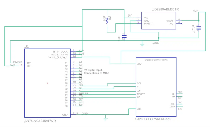
The connections between the display and the voltage level shifter are connected to prevent the digital logic voltage from exceeding 3V. The table below defines the pin connections between the display and the voltage level shifter. The pins that are required signal translation are the connections for the three wire serial communication interface.
| No. | Display | Voltage Shifter | External | Description |
| 1 | SCL | B1 | — | Level shifted digital input |
| 2 | SI | B2 | — | Level shifted digital input |
| 3 | VDD | VCCB | — | Output voltage 3.0V |
| 4 | A0 | B3 | — | Level shifted digital input |
| 5 | RESET | B4 | — | Level shifted digital input |
| 6 | CS | B5 | — | Level shifted digital input |
| 7 | VSS | GND | GND | System ground |
| 8 | H- | — | Heater ground | LCD heater ground |
| 9 | H+ | — | Heater voltage | LCD heater voltage |
| 10 | LED- | — | Backlight GND | Backlight circuit ground |
| 11 | LED+ | — | 3.0V | Backlight circuit voltage |
| 12 | NC | — | — |
Table 7: Graphic LCD Pin Connections
The voltage level translator will allow the signals to be provided to the graphic LCD from a five volt source while preventing the display driver from surpassing its maximum voltages. The signals will be kept in the range of 3.0V and vary ±0.05 volts between on and off states. The SCL signal will operate around 2MHz and will keep this frequency through the voltage level translator.
Connection Schematic
Below is the schematic for the voltage translator and the connection interfaced to the display and voltage regulator. The circuit shows how to translate a five volt input from the MCU to a 3.0V input for the graphic LCD.
DISCLAIMER
Buyers and others who are developing systems that incorporate Focus LCDs products (collectively, “Designers”) understand and agree that Designers remain responsible for using their independent analysis, evaluation and judgment in designing their applications and that Designers have full and exclusive responsibility to assure the safety of Designers’ applications and compliance of their applications (and of all Focus LCDs products used in or for Designers’ applications) with all applicable regulations, laws and other applicable requirements.
Designer represents that, with respect to their applications, Designer has all the necessary expertise to create and implement safeguards that:
(1) anticipate dangerous consequences of failures
(2) monitor failures and their consequences, and
(3) lessen the likelihood of failures that might cause harm and take appropriate actions.
Designer agrees that prior to using or distributing any applications that include Focus LCDs products, Designer will thoroughly test such applications and the functionality of such Focus LCDs products as used in such applications.

