1. Introduction
The MIPI DSI display interface operates in two modes determined by the location of the frame buffer memory. The video mode is used when the display does not provide internal memory for the display data. High resolution displays that are interfaced through the MIPI DSI protocol do not typically provide internal frame buffer memory in order to optimize the display cost. Memory can be provided externally to the display and communicated using the video mode. This application will discuss how to operate a display using the MIPI DSI video mode.

The MIPI Alliance defines the modes of operation between the display and the host processor as Display Command Set (DCS) and Display Stream Compression (DSC). The specification represents the video and command modes of the DSI protocol. The MIPI D-PHY physical layer is specified for the high-speed video link and the low power command link. The command mode can operate in both high speed and low power interfaces. The video mode of the MIPI DSI protocol can only be implemented with the high-speed link.
In the video mode the display data is sent in a continuous stream and is framed by video synchronizing events. The data is sent in high-speed data streams and the video synchronization events can occur in both high speed and low power modes. The pixel data is controlled by the host processor and not by the standard commands listed in the datasheet of the controller. The MIPI DSI video mode operates similarly to the RGB DPI protocol with horizontal and vertical sync events.
The MIPI DSI video mode is ideal for large and high-resolution displays because it does not require the display to provide internal memory. Streaming the pixel data by implementing the video mode offers a cost-effective solution for handling large amounts of display data. High resolution displays do not typically provide internal RAM for graphics data due to cost optimization.
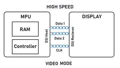
Figure 2: MIPI DSI Video Mode Interface
The display data is stored on the MCU side and streamed to the display. This requires the MCU to provide memory and operate at an efficient bandwidth to supply data to the display. The tradeoff between memory and bandwidth can be chosen based on the application and availability. Display data can be stored in portions and transmitted at greater intervals requiring a higher bandwidth.
The display used in this application is a 3.5” TFT with a 320 x 480 pixel resolution. This display is interfaced over a one data lane MIPI DSI protocol with a 20-pin FFC connector. This display can be operated in either the video or command mode because it provides internal graphic memory. The internal display memory will not be used in this application. The memory will be provided on the processor side. Additional features of this display are provided below.
| Item | Specification | Unit |
|---|---|---|
| Part No. | E35KB-FW1000-N | – |
| Display Type | TFT Active Matrix | – |
| Resolution | 320 x 480 | Pixels |
| Colors | 16.7M | Colors |
| Size | 54.46 x 82.94 | mm |
| Interface | 1-Lane MIPI DSI | – |
| Controller | ILI9488 | – |
| Mode | Transmissive | – |
| Brightness | 1000 | Nits |
2. Burst and Non-Burst Events
The video mode of the MIPI DSI communication protocol has two methods of transmitting synchronization events. The video mode uses the high-speed physical layer to communicate data in a continuous stream from the host processor to the display. The data is sent at 500Gbps for a one data lane MIPI protocol and 1Gbps for the two data lane MIPI interface.
The continuous stream of data is sent as a long packet and framed by synchronization events. The stream is composed of packed RGB pixel data in a specified color format. The data and synchronization events are similar to other video interface standards. These synchronization events can occur in burst and non-burst communication modes.
The burst mode is when the low power setting is enabled for the synchronization events. The synchronization events are sent in the short packet data type in between the pixel data bursts. The RGB data is time compressed which allows time for the high speed to low power transition.
In the burst mode, the entire active pixel region is sent in one long packet. The burst mode requires the FIFO memory to contain enough memory to support one full stream of active pixels. The stream of display data is sent in a continuous and uninterrupted stream. The display data is transmitted in one burst and then quickly returned to the low power mode.

Figure 3: MIPI DSI Video Mode Burst Events
The non-burst mode does not implement a low power sequence for every synchronization event. The non-burst most will typically integrate a low power synchronization event once per frame or as recommended by the display controller. Instead of low power synchronization events, the non-bust mode uses null or blank packets to signify a synchronization event.
The non-burst mode allows for an accurate representation of specified display timings. The non-burst mode does not require the user to specify the period of blank or null packets to signify a sync event. The null and blank packet frequency is calculated by the specified horizontal and vertical display timings.

Figure 4: MIPI DSI Video Mode Non-Burst Events
3. Synchronization and Timing Signals
The MIPI DSI video mode is similar to the RGB parallel communication protocol in that it consists of data streaming and synchronization signals. The signals are specified as timing parameters such as: HSYNC, VSYNC, and DCLK timings. The MIPI DSI protocol transmits data at 500Mbps or 1Gbps for two data lanes. The faster data transmission allows for fewer data lanes to communicate with the display.
The porch timings that are seen in other high speed display interfaces are included in the low power and blank packet events. The number of bytes is calculated to construct the length of these sync events. The following values were used to synchronize the display data.
| Symbol | Description | Value | Unit |
|---|---|---|---|
| HSYNC | Horizontal Sync Pulse Width | 2 | DCLK |
| VSYNC | Vertical Sync Pulse Width | 2 | HSYNC |
| HACT | Horizontal Active Area | 320 | DCLK |
| VACT | Vertical Active Area | 480 | HSYNC |
| HBP | Horizontal Back Porch | 34 | DCLK |
| VBP | Vertical Back Porch | 15 | HSYNC |
| HFP | Horizontal Front Porch | 34 | DCLK |
| VFP | Vertical Front Porch | 16 | HSYNC |
The minimum pixel clock speed is calculated by the display area to maintain a refresh rate of 60 fps.
Horizontal Total = 2 + 320 + 34 + 34 = 390
Vertical Total = 2 + 480 + 15 + 16 = 513
Pixel Clock = 390 x 513 x 60 = 12 MHz
The DSI minimum bandwidth required to maintain an image on the display is determined by the pixel clock and the desired color depth. The DSI protocol has a maximum bandwidth of 500Mbps.
DSI Bandwidth = Pixel Clock x Color Depth = 12 MHz x 16 bpp = 192 Mbps
Bandwidth can be adjusted by the color depth chosen and the video mode used. The burst mode can increase the bandwidth because transmission time is shortened to provide time to switch to the low power mode for the synchronization events. The color depth determines the amount of data that is required to be sent per pixel. Decreasing color depth will decrease the required bandwidth.
The pixel clock can be set to utilize the maximum DSI bandwidth at 500Mbps by calculating the pixel clock at the desired color depth.
Pixel Clock = DSI 1-lane Max BW / Color Depth = 500Mbps / 16 bpp = 31.25 MHz
4. Hardware Connection
The display is connected to the processor though one differential data pair and one differential clock pair. The signals are connected through a 20-pin ribbon cable attached to the display. The display is connected through a FFC connector and rerouted to match the pin map of the connector on the MCU.
The connection to the MCU is through a 60-pin mezzanine connector. The required pins are routed to the controller while the additional pins can be left open. The MIPI DSI port on the MCU offers additional data lanes and touch panel support. These features will not be used for this application.
The backlight of the display is powered externally from the communication interface. The backlight consists of two parallel rows with five white LEDs in series. The LEDs are powered at 15.6V and 60mA. The backlight circuit is seen below.
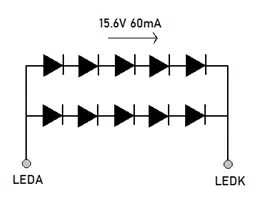
Figure 5: Backlight LED Circuit Diagram
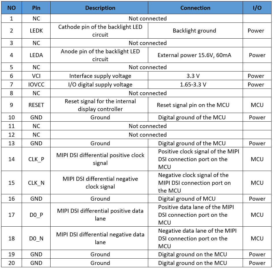
The 20 pins of the display are described in the table below. Each pin is described by the function and the connection to the MCU.
The microprocessor is a part of a development board developed by ST Microelectronics. The microcontroller has a 64-bit ARM Cortex-M4 processor and a MIPI DSI interface port. The part number for this development board is STM32L4R9AI-Discovery. This board was chosen because it has the MIPI DSI interface capabilities available for the display. This provides systems such as graphics control and memory features which would otherwise need to be provided externally.
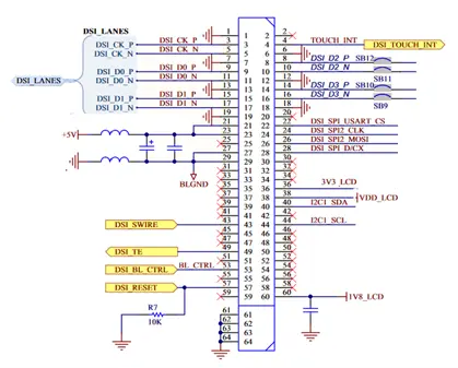
Figure 7: MIPI DSI Connector Port on STM32L4R9AI
This application applies to the processor STM32L4R9AII6 and can be reproduced without the necessity of the external MCU features. The MIPI DSI port on the MCU can support up to 4 data lanes, a backlight charge pump, and capacitive touch functionality. These features can be adapted to support other Focus LCDs MIPI TFT’s that offer capacitive touch interfaces and multiple data lane MIPI communication.
The pins used to connect the display to the MCU are routed to match the pin output of the mezzanine connector. Below is a reference of the pins that are routed from the display FPC to the Q-strip connector on the MCU.
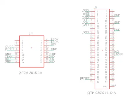
Figure 8: Display FPC Connection to MCU
5. Software Connection
The display is operated using the STM Cube IDE with the integration of the available device peripherals and HAL drivers. The features available through the STM HAL driver software include the MIPI DSI communication functions and required peripheral initialization. The required features of the microcontroller used include the LTDC, MMU, DSI PLL timings, DSI PHY timings, and frame buffer image locations.
The DSI clock configuration is set based on the calculated values determined by display type and color depth. The HAL drivers are used to enable the PLL required to generate the clock for the DSI protocol. The system clock of the controller is at 180 MHz and the pixel clock frequency will be at 12 MHz.
Below is the code example for configuring the system clock that is used to operate the controller.
DSI_PLLInitTypeDef dsiPLL;
DsiHandle.Instance = DSI;
DsiHandle.Init.AutomaticClockLaneControl = DSI_AUTO_CLK_LANE_CTRL_DISABLE;
DsiHandle.Init.TXEscapeCkdiv = 4;
DsiHandle.Init.NumberOfLanes = DSI_ONE_DATA_LANE;
dsiPLL.PLLNDIV = 125;
dsiPLL.PLLIDF = DSI_PLL_IN_DIV2;
dsiPLL.PLLODF = DSI_PLL_OUT_DIV1;
HAL_DSI_Init(&DsiHandle, &dsiPLL);
The physical timings of the DSI interface need to be specified for burst or non-burst modes. The timing values for state transitions are listed in the datasheet of the display controller. These timings define the maximum time allowed for the clock to switch from high speed to low power and vice versa.
DSI_PHY_TimerTypeDef PhyCLK;
PhyCLK.ClockLaneHS2LPTime = 28;
PhyCLK.ClockLaneLP2HSTime = 36;
PhyCLK.DataLaneHS2LPTime = 18;
PhyCLK.DataLaneLP2HSTime = 17;
PhyCLK.DataLaneMaxReadTime = 0;
PhyCLK.StopWaitTime = 0;
HAL_DSI_ConfigPhyTimer(&DsiHandle, &PhyCLK)
The video mode is then initialized for the display. This sequence specifies the synchronization parameter, packet size, burst/non-burst modes, and the color format. For this application, the burst mode will be used to transmit data to the display. The burst mode is available because of the lower resolution and less strict bandwidth limitations.
VideoMd.VirtualChannelID = 0;
VideoMd.ColorCoding = DSI_RGB565;
VideoMd.LooselyPacked = DSI_LOOSELY_PACKED_DISABLE;
VideoMd.Mode = DSI_VIDE_MODE_BURST;
VideoMd.PacketSize = 320;
VideoMd.NumberOfChunks = 0;
VideoMd.NullPacketSize = 0;
VideoMd.HSPolarity = DSI_HSYNC_ACTIVE_LOW;
VideoMd.VSPolarity = DSI_VSYNC_ACTIVE_LOW;
VideoMd.DEPolarity = DSI_DATA_ENABLE_ACTIVE_HIGH;
VideoMd.HorizontalSyncActive = 2;
VideoMd.HorizontalBackPorch = 34;
VideoMd.HorizontalLine = 390;
VideoMd.VerticalSyncActive = 2;
VideoMd.VerticalBackPorch = 15;
VideoMd.VerticalFrontPorch = 16;
VideoMd.VerticalActive = 513;
VideoMd.LPCommandEnable = DSI_LP_COMMAND_ENABLE;
VideoMd.LPLargestPacketSize = 16;
VideoMd.LPVACTLargestPacketSize = 0;
VideoMd.LPHorizontalFrontPorchEnable = DSI_LP_HFP_ENABLE;
VideoMd.LPVerticalActiveEnable = DSI_LP_VFP_ENABLE;
VideoMd.LPVerticalFrontPorchEnable = DSI_LP_VFP_ENABLE;
VideoMd.LPVeritcalBackPorchEnable = DSI_LP_VBP_ENABLE;
VideoMd.LPVerticalSyncActiveEnable = DSI_LP_VSYNC_ENABLE;
HAL_DSI_ConfigVideoMode(&DsiHandle, &VideoMd);
With the display communication settings initialized, the other on board features and drivers can be implemented to stream video to the display. The LTDC feature of the STM32 HAL drivers is responsible for controlling and formatting the data in the stream to accurately portray the image on the display.
The horizontal and vertical synchronization parameters must be consistent across the DSI host and the LTDC. The LTDC is in charge of taking image data from memory and correctly ordering it through the DSI host. This can occur in partial layers image data or updates to the full frame.
The LTDC controller acts similarly to the internal display controller in that it accesses and interacts with the display data in memory. The difference for the video mode is that the LTDC accesses memory from the processor instead of the display controlling and storing the data.
The memory location is determined based on availability. External memory sources can be integrated to conserve system memory. External memory gives availability to multiple buffering and higher color depth. The memory location for this application was chosen to be the on board SRAM. The on board SRAM provided enough memory for a full page at 16bpp color.
Methods of partial data storage and partial image refreshing can be implemented to conserve on board memory and bandwidth. The memory locations on a given board are typically broken up into variable sizes and availability. It is recommended to store the framebuffer in a location such as RAM that has a faster access time to avoid tearing or flickering of image data.
DISCLAIMER
Buyers and others who are developing systems that incorporate FocusLCDs products (collectively, “Designers”) understand and agree that Designers remain responsible for using their independent analysis, evaluation and judgment in designing their applications and that Designers have full and exclusive responsibility to assure the safety of Designers’ applications and compliance of their applications (and of all FocusLCDs products used in or for Designers’ applications) with all applicable regulations, laws and other applicable requirements.
Designer represents that, with respect to their applications, Designer has all the necessary expertise to create and implement safeguards that:
(1) anticipate dangerous consequences of failures
(2) monitor failures and their consequences, and
(3) lessen the likelihood of failures that might cause harm and take appropriate actions.
Designer agrees that prior to using or distributing any applications that include FocusLCDs products, Designer will thoroughly test such applications and the functionality of such FocusLCDs products as used in such applications.

