LCD Grounding and Return Path Design for EMI Stability in High-Speed Interfaces
What is LCD grounding and return path design?
LCD grounding and return path design refers to the control of current flow paths that support high-speed signal transmission, ensuring stable electrical performance, low electromagnetic emissions, and reliable operation in embedded display systems.
Why LCD Grounding and Return Path Design Matters in OEM Systems
LCD grounding and return path design is fundamental to achieving stable electrical performance in systems using high-speed interfaces such as MIPI DSI, RGB, and LVDS. Improper grounding introduces noise, increases electromagnetic emissions, and degrades signal integrity.
In rugged, medical, defense, and industrial systems, unstable grounding behavior can lead to intermittent failures, EMI compliance issues, and extended validation timelines.
Because of this, grounding strategy must be treated as a primary electrical design consideration within the overall system architecture.
Focus LCDs manufactures and supplies standard and custom LCD modules for OEM integration. Focus LCDs works with engineering teams to define grounding strategies, interface layouts, and integration approaches that support predictable electrical performance. Final system validation, certification, and compliance remain the responsibility of the OEM.
How Return Path Behavior Affects High-Speed LCD Signal Performance
High-speed signals do not travel in isolation.
Every signal requires a return path.
If that return path is discontinuous, high impedance, or poorly defined, several issues can occur:
• Increased radiated emissions
• Signal distortion and jitter
• Crosstalk between interfaces
• Reduced noise immunity
As a result, even well-routed differential pairs can fail if return path continuity is compromised.
These effects are closely tied to high-speed interface behavior, as discussed in MIPI DSI Signal Integrity Basics for Reliable LCD Integration.
Understanding LCD Return Path Behavior
In high-speed systems, return current follows the path of least impedance, not necessarily the shortest physical path.
For controlled impedance traces:
• Return current flows directly beneath the signal trace
• Ground plane continuity is critical
• Disruptions force current to detour, increasing loop area
Larger loop areas increase electromagnetic radiation.
Maintaining a continuous reference plane is therefore essential for EMI stability.
LCD Return Path Failure Modes and System Impact
Common return path issues directly affect signal integrity and EMI performance.
| Return Path Issue | Impact on System |
|---|---|
| Crossing ground plane splits | Increased EMI and signal distortion |
| Connector ground discontinuity | Jitter and intermittent failures |
| Large loop area | Increased radiated emissions |
| Weak or fragmented ground reference | Reduced noise immunity and signal instability |
These failure modes often appear during validation rather than initial bring-up, making early grounding design critical.
LCD Grounding Design: Good vs Poor Practices
A comparison highlights how LCD grounding and return path design affects system stability.
Good grounding design:
• Continuous ground plane under signal traces
• Tight coupling between signal and return path
• Consistent impedance across the interface
• Minimal loop area
Poor grounding design:
• Split or interrupted ground planes
• Long or indirect return paths
• Discontinuous reference across connectors
• Large loop areas that increase emissions
Even well-routed signals can fail if return path integrity is compromised.
Common LCD Grounding Challenges in High-Speed Interfaces
LCD Grounding Across Split Ground Planes
Splitting ground planes between analog, digital, or power domains is a common practice. However, when high-speed signals cross these splits:
• Return paths are interrupted
• Impedance discontinuities occur
• Noise coupling increases
As a result, signal integrity and EMI performance degrade simultaneously.
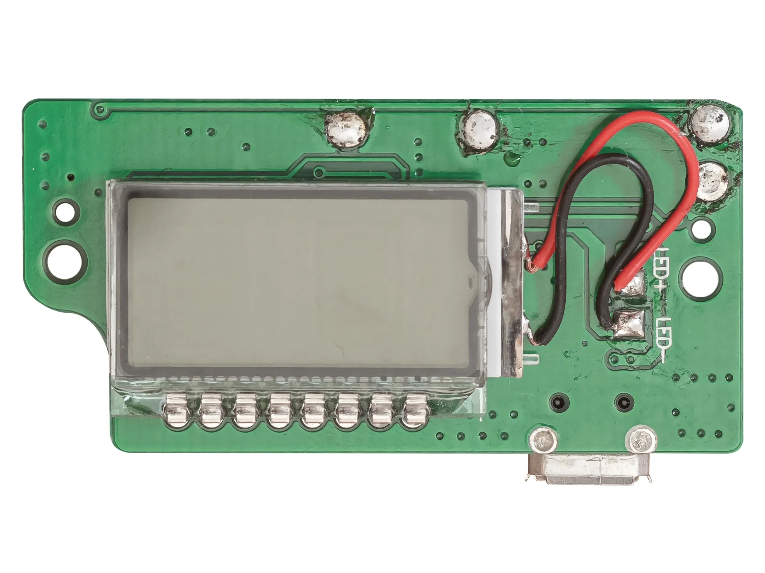
LCD Grounding at Connector and Flex Cable Transitions
LCD modules often connect via flex cables or board-to-board connectors.
At these transition points:
• Ground reference may change
• Impedance may shift
• Return path continuity may break
Focus LCDs works with OEM teams to evaluate connector selection, pin assignment, and flex layout to maintain consistent grounding across transitions. These considerations are especially important in high-speed MIPI DSI and LVDS LCD module configurations where grounding continuity directly impacts signal performance.
Incomplete LCD Ground Referencing
High-speed interfaces require solid reference planes.
When signals reference fragmented or narrow ground paths:
• Return current density increases
• Voltage fluctuations occur
• EMI emissions increase
Grounding must extend across the full signal path to maintain stability.
LCD Grounding and EMI Performance
LCD grounding and return path design directly affects electromagnetic emissions and immunity.
Poor grounding can:
• Increase radiated emissions
• Reduce shielding effectiveness
• Increase susceptibility to external interference
EMI fundamentals and compliance requirements are defined in standards such as International Electrotechnical Commission IEC.
Measurement and troubleshooting techniques are also discussed in Keysight EMI Measurement Fundamentals.
Grounding strategy must align with system-level EMC design to achieve predictable compliance outcomes.
LCD Grounding Interaction with Signal Integrity
LCD grounding and return path design is tightly coupled with signal integrity.
Even when differential pairs are:
• Properly routed
• Length matched
• Correctly terminated
Poor return path design can still degrade performance.
These interactions are further explored in EMI EMC in LCD Modules: Display-Level Design Considerations and MIPI DSI Signal Integrity Basics for Reliable LCD Integration.
Mechanical and Environmental Effects on LCD Grounding
In rugged environments, grounding stability can change over time.
Factors include:
• Vibration affecting connector contact
• Mechanical stress altering grounding paths
• Environmental exposure influencing conductivity
Because of these variables, grounding design must consider long-term stability, not just initial performance.
This becomes especially important in harsh environments, as discussed in Rugged LCD Design for Harsh and Safety-Critical Applications.
How to Design LCD Grounding for EMI Stability
Effective LCD grounding and return path design requires controlling current flow paths, maintaining continuous reference planes, and minimizing loop area to reduce emissions and improve signal integrity.
Practical LCD Grounding and Return Path Design Guidelines
Maintain continuous ground reference planes wherever possible.
Avoid routing high-speed signals across plane splits.
Ensure connector pinouts preserve ground continuity.
Keep return paths close to signal traces to minimize loop area.
Validate grounding behavior during EMI testing rather than relying on assumptions.
LCD Grounding Design Checklist for EMI Stability
Engineers can use the following checklist to verify grounding effectiveness:
• Continuous ground plane beneath all high-speed signal traces
• No high-speed routing across ground plane splits
• Ground continuity maintained across connectors and flex interfaces
• Minimal loop area between signal and return paths
• Stable grounding under mechanical and environmental stress
• Validation through EMI testing and measurement
Focus LCDs Engineering Approach
Focus LCDs manufactures and supplies standard and custom LCD modules and works with OEM engineering teams to define interface layouts, grounding strategies, and mechanical integration approaches that support stable electrical performance.
By aligning grounding, signal integrity, and mechanical design early in development, Focus LCDs helps reduce integration risk and improve validation outcomes in long-lifecycle and regulated systems.
Scope Boundary and Compliance Responsibility
Focus LCDs provides LCD modules and engineering support for integration. Focus LCDs does not control final system grounding architecture, EMI mitigation strategy, or regulatory certification.
OEMs remain responsible for validating compliance within their complete system design.
Contact Focus LCDs
If you are developing a system where EMI stability and high-speed interface reliability are critical, Focus LCDs can supply standard or custom LCD modules and assist with grounding strategy, interface planning, and integration.
Contact Focus LCDs:
https://focuslcds.com/contact
FAQ: LCD Grounding and Return Path Design
What is a return path in LCD design?
A return path is the path through which current flows back to its source, typically through a ground plane beneath signal traces.
Why is grounding important for EMI?
Proper grounding minimizes loop area, reduces electromagnetic emissions, and improves noise immunity.
What happens if return path continuity is broken?
Signal distortion, increased EMI, and unstable system behavior can occur.
Do differential signals eliminate grounding concerns?
No. Differential signals reduce noise sensitivity but still rely on stable return paths for optimal performance.
Conclusion: LCD Grounding Defines Electrical Stability
LCD grounding and return path design are foundational to reliable LCD integration.
Without a continuous and controlled return path, high-speed interfaces become unpredictable, EMI performance degrades, and system validation becomes more difficult.
In high-reliability systems, stable electrical behavior begins with disciplined grounding design.

